- 您现在的位置:买卖IC网 > Sheet目录1201 > CDB5461AU (Cirrus Logic Inc)BOARD EVAL & SOFTWARE CS5461A
�� �
�
�CS5461A�
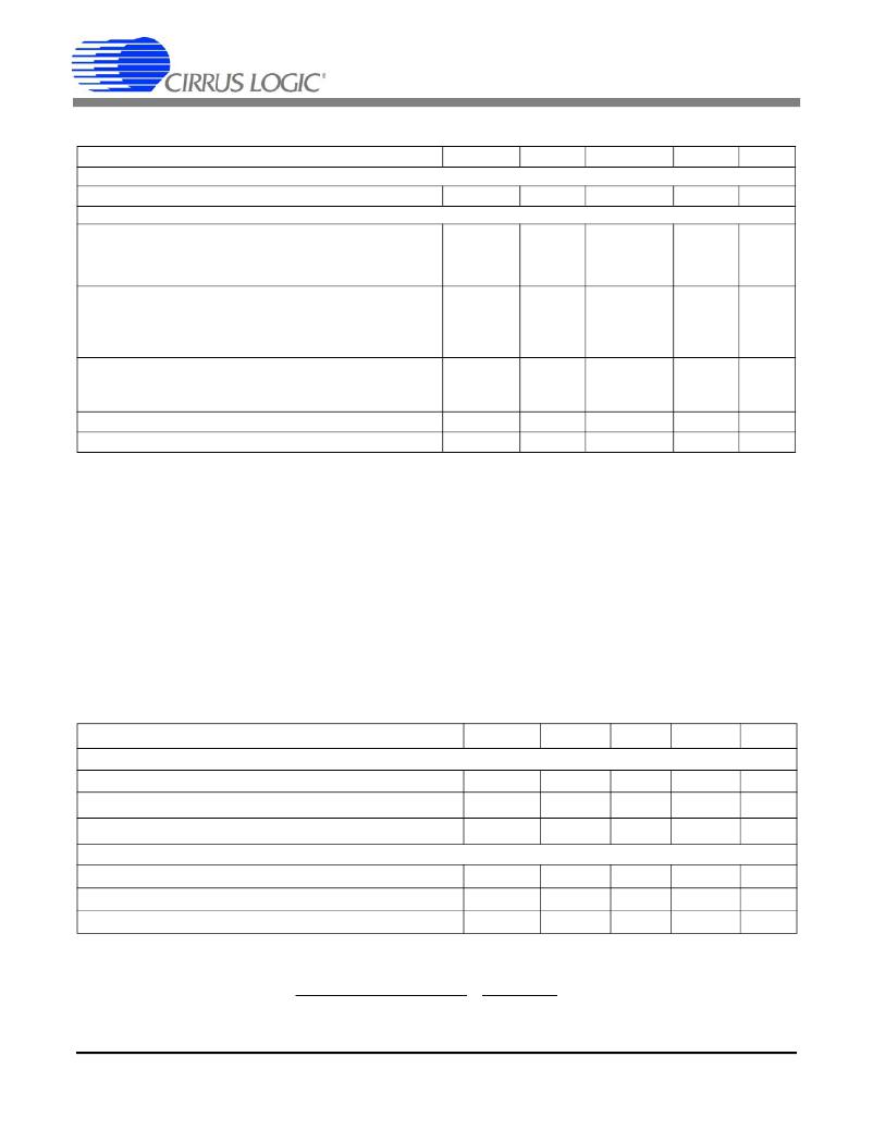
�ANALOG� CHARACTERISTICS� (Continued)�
�Parameter�
�Symbol�
�Min�
�Typ�
�Max�
�Unit�
�Temperature� Channel�
�Temperature� Accuracy�
�T�
�-�
�±5�
�-�
�°C�
�Power� Supplies�
�Power� Supply� Currents� (Active� State)� I� A+�
�I� D+� (VA+� =� VD+� =� 5� V)�
�I� D+� (VA+� =� 5� V,� VD+� =� 3.3� V)�
�Power� Consumption� Active� State� (VA+� =� VD+� =� 5� V)�
��Stand-By� State�
�Sleep� State�
�PSCA�
�PSCD�
�PSCD�
�PC�
�-�
�-�
�-�
�-�
�-�
�-�
�-�
�1.1�
�2.9�
�1.7�
�21�
�12�
�8�
�10�
�-�
�-�
�-�
�28�
�16.5�
�-�
�-�
�mA�
�mA�
�mA�
�mW�
�mW�
�mW�
�μW�
�Power� Supply� Rejection� Ratio� (DC,� 50� and� 60� Hz)�
��Current� Channel�
���PSRR�
�PMLO�
�PMHI�
�45�
�70�
�2.3�
�-�
�65�
�75�
�2.45�
�2.55�
�-�
�-�
�-�
�2.7�
�dB�
�dB�
�V�
�V�
�PSRR� =� 20� ?� log� ?� ----------� ?�
�1.� Applies� when� the� HPF� option� is� enabled.�
�2.� Applies� before� system� calibration.�
�3.� All� outputs� unloaded.� All� inputs� CMOS� level.�
�4.� Measurement� method� for� PSRR:� VREFIN� tied� to� VREFOUT,� VA+� =� VD+� =� 5� V,� a� 150� mV� (zero-to-peak)� (60� Hz)�
�sinewave� is� imposed� onto� the� +5� V� DC� supply� voltage� at� VA+� and� VD+� pins.� The� “+”� and� “-”� input� pins� of� both� input�
�channels� are� shorted� to� AGND.� Then� the� CS5461A� is� commanded� to� continuous� conversion� acquisition� mode,� and�
�digital� output� data� is� collected� for� the� channel� under� test.� The� (zero-to-peak)� value� of� the� digital� sinusoidal� output�
�signal� is� determined,� and� this� value� is� converted� into� the� (zero-to-peak)� value� of� the� sinusoidal� voltage� (measured�
�in� mV)� that� would� need� to� be� applied� at� the� channel’s� inputs,� in� order� to� cause� the� same� digital� sinusoidal� output.�
�This� voltage� is� then� defined� as� Veq.� PSRR� is� then� (in� dB)� :�
�?� 150� ?�
�?� V� eq� ?�
�5.� When� voltage� level� on� PFMON� is� sagging,� and� LSD� bit� is� at� 0,� the� voltage� at� which� LSD� bit� is� set� to� 1.�
�6.� If� the� LSD� bit� has� been� set� to� 1� (because� PFMON� voltage� fell� below� PMLO),� this� is� the� voltage� level� on� PFMON� at�
�which� the� LSD� bit� can� be� permanently� reset� back� to� 0.�
�VOLTAGE� REFERENCE�
�Parameter�
�Symbol�
�Min�
�Typ�
�Max�
�Unit�
�Reference� Output�
�Output� Voltage�
�VREFOUT�
�+2.4�
�+2.5�
�+2.6�
�V�
�Temperature� Coefficient�
�Load� Regulation�
���TC� VREF�
�?� V� R�
�-�
�-�
�25�
�6�
�60�
�10�
�ppm/°C�
�mV�
�Reference� Input�
�Input� Voltage� Range�
�Input� Capacitance�
�Input� CVF� Current�
�VREFIN�
�+2.4�
�-�
�-�
�+2.5�
�4�
�25�
�+2.6�
�-�
�-�
�V�
�pF�
�nA�
�Notes:� 7.� The� voltage� at� VREFOUT� is� measured� across� the� temperature� range.� From� these� measurements� the� following�
�formula� is� used� to� calculate� the� VREFOUT� Temperature� Coefficient:.�
�(� (� V� R� E� F� O� V� R� E� F� O� U� T� R� E� F� O� U� T�
�TC�
�VREF�
�=�
�UT� MAX� -� V�
�AVG�
�M� IN� )�
�(� T�
�A�
�M� AX�
�1�
�-� T� A� M� IN�
�(� 1� .0�
�x� 10�
�6�
�8�
�8.�
�Specified� at� maximum� recommended� output� of� 1� μA,� source� or� sink.�
�DS661F3�
�发布紧急采购,3分钟左右您将得到回复。
相关PDF资料
CDB5466U
BOARD EVAL & SOFTWARE CS5466 ADC
CDB5467U
BOARD EVAL FOR CS5467 ADC
CDB5560-2
DEV BOARD FOR CS5560 W/SE INPUT
CDB5571-2
DEV BOARD FOR CS5571 W/SE INPUT
CDB8422
BOARD EVAL FOR CS8422 RCVR
CDB8952T
BOARD EVAL FOR CS8952
CDCE906-706PERFEVM
EVAL MOD PERFORMANCE CDCE906/706
CEVAL-033
BOARD EVAL FOR CVCO33 .3"X.3"
相关代理商/技术参数
CDB5461AU-Z
制造商:Cirrus Logic 功能描述:PB-FREEEVAL BOARD FOR CS5461 WITH USB - Bulk
CDB5462
制造商:Cirrus Logic 功能描述:EVAL BOARD FOR CS5462 - Bulk
CDB5463U
功能描述:数据转换 IC 开发工具 Eval Bd Sngl-Phase Pow/Energy
RoHS:否 制造商:Texas Instruments 产品:Demonstration Kits 类型:ADC 工具用于评估:ADS130E08 接口类型:SPI 工作电源电压:- 6 V to + 6 V
CDB5463U-Z
功能描述:EVAL BOARD USB FOR CS5463 RoHS:是 类别:编程器,开发系统 >> 评估板 - 模数转换器 (ADC) 系列:- 产品培训模块:Obsolescence Mitigation Program 标准包装:1 系列:- ADC 的数量:1 位数:12 采样率(每秒):94.4k 数据接口:USB 输入范围:±VREF/2 在以下条件下的电源(标准):- 工作温度:-40°C ~ 85°C 已用 IC / 零件:MAX11645 已供物品:板,软件
CDB5464U
功能描述:数据转换 IC 开发工具 Eval Bd 3-Ch Sngl-Phs Pow/Energy
RoHS:否 制造商:Texas Instruments 产品:Demonstration Kits 类型:ADC 工具用于评估:ADS130E08 接口类型:SPI 工作电源电压:- 6 V to + 6 V
CDB5464U-Z
制造商:Cirrus Logic 功能描述:EVAL BD PB-FREE DEMO BOARD FOR CS5464 - Boxed Product (Development Kits) 制造商:Cirrus Logic 功能描述:Eval Board
CDB5466U
功能描述:数据转换 IC 开发工具 Eval Bd F/Residental Pow-Meter Apps
RoHS:否 制造商:Texas Instruments 产品:Demonstration Kits 类型:ADC 工具用于评估:ADS130E08 接口类型:SPI 工作电源电压:- 6 V to + 6 V
CDB5466U-Z
制造商:Cirrus Logic 功能描述:PB-FREEEVAL BOARD FOR CS5466 WITH USB - Bulk